Why SPI matters
If you have ever opened a sensor datasheet and seen the words "three-wire interface", "synchronous serial", or simply "SPI compatible", you have met the Serial Peripheral Interface. SPI is, in the systems I design, the workhorse bus for anything that needs to move data quickly between a microcontroller and a nearby chip: flash memories, displays, high-resolution ADCs, IMUs, SD cards, and dedicated radio chips. It is not the newest protocol, and it has no built-in acknowledgment mechanism, but it is fast, cheap, deterministic, and simple enough that you can debug it with a two-channel oscilloscope.
By the end of this tutorial you will understand SPI at the level of individual signal edges, be able to read an SPI timing diagram from any datasheet, know the classic failure modes (and how to avoid them), and have built a real two-board master/slave system with working firmware on both sides. No prior knowledge of SPI is assumed — we start from zero.
The fundamentals: what SPI actually is
SPI is a synchronous, full-duplex, master/slave serial bus. Let us unpack each word, because each one carries design consequences.
- Serial: one bit at a time travels on a single data line, as opposed to parallel buses that move 8 or 16 bits simultaneously on 8 or 16 wires. Fewer pins, lower cost — at the price of needing more clock edges to move the same data.
- Synchronous: a separate clock line tells the receiver exactly when each bit is valid. There is no baud rate to guess, no start or stop bits. The sender and receiver share the clock, so the data rate is simply whatever the master clocks at — from a few kilohertz up to tens or even a hundred megahertz on modern chips.
- Full-duplex: data moves in both directions on separate lines during the same clock transaction. Every SPI transfer is inherently an exchange: as the master shifts a bit out, a bit comes back in. You cannot avoid receiving — even if you only send, a byte comes back (often garbage).
- Master/slave: exactly one device, the master, generates the clock and initiates every transaction. All other devices are slaves that only respond. SPI has no arbitration and no multi-master specification in common practice.
The reason SPI is so fast and simple is precisely what it lacks: no addressing inside the protocol, no acknowledgments, no CRC. All discipline — chip selection, framing, error checking — is the designer's responsibility. That is the central trade-off of this whole tutorial: SPI gives you speed and simplicity, and in exchange you provide the protocol discipline.
The four wires
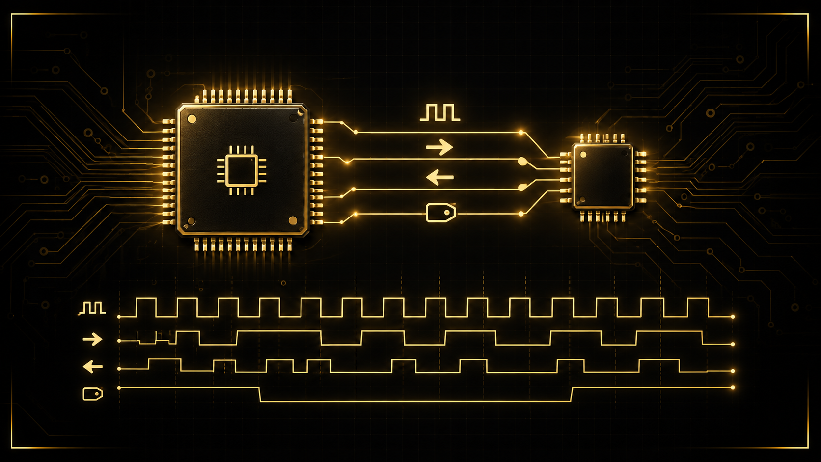
A standard SPI bus uses four signals. You will also see the older Motorola names, since Motorola invented SPI in the mid-1980s for their 68000-series microcontrollers:
Master                          Slave
              SCLK ──────────────────►  SCLK    (clock, from master only)
              MOSI ──────────────────►  MOSI    (master out, slave in)
              MISO ───────────────────  MISO    (master in, slave out)
              CS/SS ─────────────────►  CS/SS   (chip select, active low)
- SCLK (Serial Clock): generated only by the master. Every clock edge (or pair of edges, depending on mode) moves one bit.
- MOSI (Master Out, Slave In): data from master to slave. Also called SDO on some chips — always check which naming a datasheet uses relative to your device's role.
- MISO (Master In, Slave Out): data from slave to master.
- CS/SS (Chip Select / Slave Select): one dedicated line per slave, driven low to select the device. This is not a clock-line companion; it is the framing signal that tells a slave "this transaction is for you".
Note that CS is active low by long-standing convention. When CS is high, a well-behaved slave puts its MISO pin into a high-impedance state so it does not fight other slaves on the shared MISO line.
How a transfer works, edge by edge
Inside both devices sits a shift register — typically 8 bits. The two shift registers are effectively connected as a ring: master's output feeds slave's input and vice versa. On each clock pulse, both registers shift one bit. After eight clocks, the master has received what the slave had, and the slave has received what the master had. This is why every SPI read is also a write: to read a register from a sensor you usually have to send a command byte first, and during that byte the data the slave shifts back is often a dummy byte you discard.
A typical read transaction looks like this:
CS ────┐                                      ┌────────
       └──────────────────────────────────────┘
        (low = selected for the whole transaction)

SCLK    ___     ___     ___     ___     ___
     __/   \___/   \___/   \___/   \___/   \___      ...16 clocks

MOSI   <-- READ cmd (8 bits) --><-- dummy 0x00 ------->
MISO   <-- don't care ---------><-- register value -->
The master asserts CS low, clocks out the command byte while ignoring what comes back, then clocks a dummy byte out (often 0x00 or 0xFF — check the datasheet; some devices require 0xFF so the master's line can also serve a pull-up role) while the slave drives the answer onto MISO. Then CS returns high, ending the frame.
Clock polarity and clock phase (CPOL/CPHA)
This is the topic that confuses more newcomers than anything else in SPI, so we will take it slowly.
The SPI standard does not define a single clocking convention — it defines four, selected by two bits:
- CPOL (Clock Polarity): the idle level of SCLK. CPOL = 0 means the clock idles low; CPOL = 1 means it idles high.
- CPHA (Clock Phase): which clock edge latches (samples) the data. CPHA = 0 samples on the leading (first) edge of the pulse; CPHA = 1 samples on the trailing (second) edge. "Leading" and "trailing" are defined relative to the pulse shape, so for CPOL = 0 the leading edge is rising and for CPOL = 1 it is falling.
The four combinations are called SPI modes 0 through 3:
| Mode | CPOL | CPHA | SCLK idle | Data sampled | Data shifted |
|---|---|---|---|---|---|
| 0 | 0 | 0 | Low | Rising edge | Falling edge |
| 1 | 0 | 1 | Low | Falling edge | Rising edge |
| 2 | 1 | 0 | High | Falling edge | Rising edge |
| 3 | 1 | 1 | High | Rising edge | Falling edge |
The why behind the modes: with CPHA = 0, the slave must put the first data bit on the line before the first clock edge arrives — in fact it must drive MOSI/MISO as soon as CS falls. Some devices cannot react that quickly to CS, and for those the designer uses CPHA = 1, which gives the slave half a clock period after the leading edge to present data. That is the entire practical meaning of phase: it moves the sampling point by one half-clock so that data has time to settle.
How to choose the right mode: do not guess. The device datasheet tells you, either explicitly ("SPI mode 0", "CPOL = 0, CPHA = 0") or via a timing diagram — look at the clock's idle level (that is CPOL) and at which edge the "sampling" arrow sits (that is CPHA). A very common symptom of a wrong mode is reading shifted data: a byte that should be 0x80 appears as 0x01 or 0x40, because every bit was latched one edge too early or too late. When I bring up an unknown SPI board, trying all four modes is a five-minute experiment that has saved me days.
Chip select: the underrated signal
Beginners treat CS as a mere "on/off" line. In reality CS does three jobs:
- Addressing: with one CS per slave, the master selects whom it talks to. This is SPI's only addressing mechanism.
- Framing: CS going low tells the slave "a transaction begins now"; CS going high ends it and typically resets the slave's internal bit counter and command state machine. Without clean CS edges, a slave that lost sync stays lost.
- Bus release: CS high forces the slave's MISO output to high impedance, so multiple slaves can share one MISO line.
Practical consequences: keep CS asserted for an entire multi-byte transaction (do not toggle it between bytes unless the datasheet says to); in software, drive CS as a normal GPIO, not through the SPI peripheral's automatic control, so you control framing exactly; and when bit-banging, change MOSI only when the datasheet's setup-time allows (for CPHA = 0, MOSI must be valid before the first clock edge).
Bus topology and electrical considerations
The classic topology is one master with independent CS lines to each slave, all sharing SCLK, MOSI and MISO:
             ┌──────── CS1 ──► Flash
Master ──SCLK┼── CS2 ──► Sensor
   MOSI/MISO ┴─ shared by all slaves
Points that matter electrically:
- Trace length and signal integrity: SPI has no defined maximum bus length. At a few hundred kilohertz you can run it across a house; at 20+ MHz, keep leads short (a few centimetres to tens of centimetres) and treat it as a transmission-line problem. Ground return paths matter — route each signal with a nearby ground.
- Pull-ups: SPI is a push-pull protocol; it does not need pull-up resistors like I2C. A weak pull-up on CS can still be wise so that a slave is not spuriously selected while the master boots and its pins float.
- Logic levels: a 5 V master and a 3.3 V flash chip will destroy the chip. Use level shifters or run everything at one voltage. Many Arduino boards are 5 V logic; most modern sensors are 3.3 V — in the project below I specify a 3.3 V-capable setup for exactly this reason.
- Series resistors: 22–100 Ω in series with SCLK/MOSI/MISO tame ringing and EMI on longer lines. One of my standard review checks on client boards.
SPI versus I2C and UART
| SPI | I2C | UART | |
|---|---|---|---|
| Wires | 4 + 1 per extra slave | 2 (shared bus) | 2 (point-to-point) |
| Typical speed | Up to tens of MHz | 100 kHz / 400 kHz / 1 MHz / 3.4 MHz modes | Up to ~1–5 Mbaud typical |
| Addressing | Hardware CS lines | 7-/10-bit software address | None (point-to-point) |
| Acknowledgment | None | ACK/NACK per byte | Optional parity only |
| Full duplex | Yes | No (single data line) | Yes |
| Best for | Fast, local, one-to-few | Many slow devices, two pins | Two devices, async links |
The rule of thumb I use: SPI when speed or deterministic timing matters and pins are available; I2C when there are many slow devices and pins are scarce; UART for links between two systems or across longer cables with a rugged transceiver such as RS-485.
DMA, interrupts and throughput
Polling a byte at a time wastes CPU cycles. Real firmware typically uses the SPI peripheral's interrupt or (better) DMA: you set up a buffer, start the transfer, and the CPU does other work until the completion callback fires. On STM32, ESP32 and i.MX-class chips I always wire SPI to DMA for anything over a few hundred bytes — display framebuffer updates and flash reads become effectively free. We keep the project below simple (polling) for clarity, but be aware that the production step-up is DMA, not a faster polling loop.
Common mistakes and how to diagnose them
- Wrong SPI mode: bit-shifted data. Try all four modes.
- Too fast a clock: works at 1 MHz, corrupt at 10 MHz. Drop to 100 kHz during bring-up, then raise.
- Toggling CS mid-transaction: resets the slave's command state machine; reads return wrong registers.
- Ignoring the received byte: every transfer is an exchange — read what comes back even when sending.
- Not waiting for the device: flash chips and sensors need busy time after writes/commands (a status-register busy bit usually tells you). Poll it.
- Floating CS during boot: slave sees garbage clocks and locks up its state machine; add a pull-up to CS.
- Level mismatch: 5 V into a 3.3 V part — silent, permanent damage.
Diagnosis tools, in order of cost: print the raw bytes (is it shifted, zero, or 0xFF?); a two-channel scope on SCLK + MOSI or CS; and finally a cheap logic analyzer with sigrok/PulseView protocol decoding — for the money, nothing else comes close when you do the kind of work I do.
Hands-on project: an SPI master/slave link between two Arduinos
We will build the two natural sides of SPI ourselves: an Arduino Uno as master and a second Arduino (a Nano or another Uno) as a hardware SPI slave. The slave acts like a tiny sensor peripheral: it exposes a command protocol over SPI — a "who am I" query, a LED toggle, and an on-chip counter the master can read. This mirrors exactly how a real sensor works: command byte in, data byte out.
Wiring
Master (Uno)        Slave (Uno/Nano)
D13 SCLK ─────────► D13 SCLK
D11 MOSI ─────────► D11 MOSI
D12 MISO ─────────► D12 MISO
D10 CS   ─────────► D10 SS
GND ─────────────── GND            (mandatory common ground!)
Both boards are 5 V logic, so no level shifting is needed. On the Uno and Nano, the hardware SPI pins are fixed: D13 = SCLK, D11 = MOSI, D12 = MISO, D10 = SS. (On the ATmega328P these correspond to the PB5, PB3, PB4 and PB2 pins of port B.)
The slave protocol
Command byte sent by master      Byte returned by slave
0x01  WHO_AM_I  query        ->   0xA5 (fixed identity)
0x02  READ_COUNTER           ->   counter value (increments per read)
0x03  TOGGLE_LED             ->   0x00 (ack; LED on the slave toggles)
anything else               ->   0xEE (error indicator)
On AVR, hardware SPI slaves are implemented through the SPI interrupt: the SPI_STC_vect interrupt service routine fires after each completed byte. The classic pattern is to preload the answer to the next byte into SPDR, because full-duplex means the reply must already be shifted out while the next command is coming in.
Slave code (upload to the second Arduino)
// SPI Slave: pseudo-sensor peripheral (Arduino Uno/Nano, ATmega328P)
#include <avr/interrupt.h>
#include <avr/io.h>

#define CMD_WHO_AM_I   0x01
#define CMD_READ_COUNT 0x02
#define CMD_TOGGLE_LED 0x03
#define WHO_AM_I_ID    0xA5
#define ERR_CODE       0xEE

volatile uint8_t counter = 0;

// Called after every completed byte transfer.
ISR(SPI_STC_vect) {
  uint8_t cmd = SPDR;      // byte just received from master
  uint8_t reply = ERR_CODE;

  switch (cmd) {
    case CMD_WHO_AM_I:
      reply = WHO_AM_I_ID;
      break;
    case CMD_READ_COUNT:
      reply = counter++;
      break;
    case CMD_TOGGLE_LED:
      PORTB ^= _BV(PB5);   // toggle built-in LED (D13 is also SCLK...
      reply = 0x00;        // ...so on boards where the LED sits on SCLK
      break;               // use an external LED on another pin instead.
    default:
      reply = ERR_CODE;
  }
  SPDR = reply;            // preload answer for the NEXT byte
}

void setup() {
  // Built-in LED on D13 doubles as SCLK on an Uno, so for a visible
  // demo wire an external LED (with ~470R resistor) from D5 to GND:
  pinMode(5, OUTPUT);

  // Configure pins: MISO output, SCLK/MOSI/SS inputs.
  pinMode(MISO, OUTPUT);
  SPCR |= _BV(SPE);        // enable SPI in slave mode
  SPI.attachInterrupt();   // enables the SPI_STC_vect interrupt
}

void loop() {
  // Everything happens in the interrupt; mirror the LED state here
  // if you used the external-LED variant.
  digitalWrite(5, digitalRead(SCK));
}
Important note on the LED: on an Uno the built-in LED shares pin D13 with SCLK, so toggling it directly would corrupt the clock. The code above notes this and recommends an external LED on D5 — this is exactly the kind of pin-sharing trap you hit on real hardware, so I left it visible rather than hiding it.
Master code (upload to the first Arduino)
// SPI Master: queries the slave peripheral (Arduino Uno)
#include <SPI.h>

#define CMD_WHO_AM_I   0x01
#define CMD_READ_COUNT 0x02
#define CMD_TOGGLE_LED 0x03

const uint8_t CS_PIN = 10;

// Send one command byte and return the byte the slave shifted back.
// Mode 0, MSB first, <= 1 MHz to be safe with wiring and level length.
uint8_t spiTransfer(uint8_t cmd) {
  uint8_t reply;
  digitalWrite(CS_PIN, LOW);        // CS low: transaction begins
  reply = SPI.transfer(cmd);        // full-duplex: send cmd, get reply
  digitalWrite(CS_PIN, HIGH);       // CS high: transaction ends
  return reply;
}

void setup() {
  Serial.begin(115200);
  pinMode(CS_PIN, OUTPUT);
  digitalWrite(CS_PIN, HIGH);       // idle high (CS is active low)

  SPI.begin();
  SPI.beginTransaction(SPISettings(1000000, MSBFIRST, SPI_MODE0));

  uint8_t id = spiTransfer(CMD_WHO_AM_I);
  Serial.print(F("WHO_AM_I: 0x"));
  Serial.println(id, HEX);
  if (id != 0xA5) {
    Serial.println(F("Slave did not answer correctly - check wiring/mode!"));
  }
}

void loop() {
  uint8_t count = spiTransfer(CMD_READ_COUNT);
  Serial.print(F("Counter: "));
  Serial.println(count);

  spiTransfer(CMD_TOGGLE_LED);
  delay(1000);
}
What you should see
Open the serial monitor at 115200 baud. The master first prints WHO_AM_I: 0xA5 — proof the whole round-trip works — then prints an incrementing counter once per second while the slave's LED blinks. If you see 0x0 or 0xFF, check that CS actually reaches D10 on the slave and that grounds are common. If you see 0xA5 but shifted (e.g. 0x52 or 0x4A-like patterns), you have a mode problem — experiment with the other SPI_MODE values.
Experiments to deepen your understanding
- Raise the clock in
SPISettingsstep by step and find where your wiring stops working. - Remove the CS wire and observe the chaos — this is what an unframed bus looks like.
- Add a second slave with its own CS line on pin 9 and address both.
- Replace the master's polling with the
SPI.transfer(buffer, size)buffered form. - If you have a logic analyzer, capture a transaction and decode it in PulseView — matching the decoded bytes to the timing diagram is the moment SPI really clicks.
Best practices checklist
- Wrap every transaction in explicit CS low/high — never rely on automatic CS unless you have verified its behaviour.
- Use
SPI.beginTransaction()/endTransaction()(Arduino) or the equivalent peripheral configuration on your platform, so settings are consistent and interrupt-safe. - Start slow during bring-up; speed up only after correctness is proven.
- Always poll device busy flags before the next command when the datasheet requires it.
- Validate data at the application layer (CRC or sanity ranges) because SPI will not do it for you.
- Document the SPI mode, bit order and max clock next to every device driver you write — future-you will thank present-you.
A realistic learning path
- Master this project: two boards, all commands working, all modes understood.
- Talk to a real peripheral chip — a 25-series EEPROM or a W25Q flash — reading its JEDEC ID, then reading and writing pages.
- Drive a display (an ILI9341 TFT) with DMA-based block transfers; study throughput.
- Move to a bare-metal platform (STM32 HAL or register-level) and implement SPI plus its DMA stream yourself.
- Learn to read and write datasheet timing numbers (setup/hold, clock-to-output) and design to them with margin.
Conclusion
SPI rewards understanding. Once the four signals, the four modes and the role of chip select are truly clear, every SPI device datasheet becomes readable, and every bus problem becomes a short, systematic debugging session instead of guesswork. The protocol gives you almost nothing — no addressing beyond wires, no acknowledgment, no error checking — and that austerity is exactly why it is so fast and so dependable when you bring your own discipline. Build the project, break it deliberately, watch it on a scope or analyzer, and you will come out the other side genuinely fluent in one of embedded engineering's most enduring interfaces.
If you are working on an SPI-based design, debugging a stubborn bus, or want help architecting the firmware side of your next embedded product, get in touch — this is exactly the kind of work I do, and I enjoy the hard cases.